DFT TELECOM
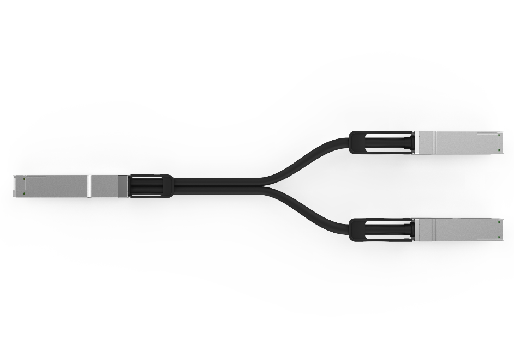
200G QSFP-DD-2xQSFP28 Direct Attach Cable (DAC)
200G QSFP-DD-2xQSFP28 Direct Attach Cable (DAC)
픽업 사용 가능 여부를 로드할 수 없습니다.
QSFP-DD-2xQSFP28 passive copper cable assembly feature sixteen differential copper pairs, providing eight data transmission channels at speeds up to 25Gbps(NRZ) per channel, and meets 200G Ethernet and InfiniBand Enhanced Data Rate(EDR) requirements. Available in a broad range of wire gages from 28AWG through 30AWG, this 200G copper cable assembly features low insertion loss and low crosstalk.

Features and Benefits
l Compatible with IEEE 802.3bj
l Supports aggregate data rates of 200Gbps(NRZ)
l Optimized construction to minimize insertion loss and crosstalk
l Pull-to-release slide latch design
l Straight and break out assembly configurations available
l Customized cable braid termination limits EMI radiation
l Customizable EEPROM mapping for cable signature
l 28AWG through30AWG cable
l 3.3V Power supply
l Temperature Range: 0~ 70 °C
l RoHS Compliant
Product Applications
l Switches, servers and routers
l Data Center networks
l Storage area networks
l High performance computing
l Telecommunication and wireless infrastructure
l Medical diagnostics and networking
l Test and measurement equipment
Industry Standards
l 200_2x100G Ethernet(IEEE 802.3bj)
l InfiniBand EDR
Pin Descriptions
QSFP-DD Pin Function Definition
|
Pin |
Logic |
Symbol |
Description |
|
1 |
|
GND |
Ground |
|
2 |
CML-I |
Tx2n |
Transmitter Inverted Data Input |
|
3 |
CML-I |
Tx2p |
Transmitter Non-Inverted Data Input |
|
4 |
|
GND |
Ground |
|
5 |
CML-I |
Tx4n |
Transmitter Inverted Data Input |
|
6 |
CML-I |
Tx4p |
Transmitter Non-Inverted Data Input |
|
7 |
|
GND |
Ground |
|
8 |
LVTTL-I |
ModSelL |
Module Select |
|
9 |
LVTTL-I |
ResetL |
Module Reset |
|
10 |
|
Vcc Rx |
+3.3V Power Supply Receiver |
|
11 |
LVCMOS- I/O |
SCL |
2-wire serial interface clock |
|
12 |
LVCMOS- I/O |
SDA |
2-wire serial interface data |
|
13 |
|
GND |
Ground |
|
14 |
CML-O |
Rx3p |
Receiver Non-Inverted Data Output |
|
15 |
CML-O |
Rx3n |
Receiver Inverted Data Output |
|
16 |
|
GND |
Ground |
|
17 |
CML-O |
Rx1p |
Receiver Non-Inverted Data Output |
|
18 |
CML-O |
Rx1n |
Receiver Inverted Data Output |
|
19 |
|
GND |
Ground |
|
20 |
|
GND |
Ground |
|
21 |
CML-O |
Rx2n |
Receiver Inverted Data Output |
|
22 |
CML-O |
Rx2p |
Receiver Non-Inverted Data Output |
|
23 |
|
GND |
Ground |
|
24 |
CML-O |
Rx4n |
Receiver Inverted Data Output |
|
25 |
CML-O |
Rx4p |
Receiver Non-Inverted Data Output |
|
26 |
|
GND |
Ground |
|
27 |
LVTTL-O |
ModPrsL |
Module Present |
|
28 |
LVTTL-O |
IntL |
Interrupt |
|
29 |
|
Vcc Tx |
+3.3V Power supply transmitter |
|
30 |
|
Vcc1 |
+3.3V Power supply |
|
31 |
LVTTL-I |
LPMode |
Low Power Mode |
|
32 |
|
GND |
Ground |
|
33 |
CML-I |
Tx3p |
Transmitter Non-Inverted Data Input |
|
34 |
CML-I |
Tx3n |
Transmitter Inverted Data Input |
|
35 |
|
GND |
Ground |
|
36 |
CML-I |
Tx1p |
Transmitter Non-Inverted Data Input |
|
37 |
CML-I |
Tx1n |
Transmitter Inverted Data Input |
|
38 |
|
GND |
Ground |
|
39 |
|
GND |
Ground |
|
40 |
CML-I |
Tx6n |
Transmitter Inverted Data Input |
|
41 |
CML-I |
Tx6p |
Transmitter Non-Inverted Data Input |
|
42 |
|
GND |
Ground |
|
43 |
CML-I |
Tx8n |
Transmitter Inverted Data Input |
|
44 |
CML-I |
Tx8p |
Transmitter Non-Inverted Data Input |
|
45 |
|
GND |
Ground |
|
46 |
|
Reserved |
|
|
47 |
|
VS1 |
|
|
48 |
|
VccRx1 |
+3.3V Power supply |
|
49 |
|
VS2 |
|
|
50 |
|
VS3 |
|
|
51 |
|
GND |
Ground |
|
52 |
CML-O |
Rx7p |
Receiver Non-Inverted Data Output |
|
53 |
CML-O |
Rx7n |
Receiver Inverted Data Output |
|
54 |
|
GND |
Ground |
|
55 |
CML-O |
Rx5p |
Receiver Non-Inverted Data Output |
|
56 |
CML-O |
Rx5n |
Receiver Inverted Data Output |
|
57 |
|
GND |
Ground |
|
58 |
|
GND |
Ground |
|
59 |
CML-O |
Rx6n |
Receiver Inverted Data Output |
|
60 |
CML-O |
Rx6p |
Receiver Non-Inverted Data Output |
|
61 |
|
GND |
Ground |
|
62 |
CML-O |
Rx8n |
Receiver Inverted Data Output |
|
63 |
CML-O |
Rx8p |
Receiver Non-Inverted Data Output |
|
64 |
|
GND |
Ground |
|
65 |
|
NC |
|
|
66 |
|
Reserved |
|
|
67 |
|
VccTx1 |
+3.3V Power supply |
|
68 |
|
VCC2 |
+3.3V Power supply |
|
69 |
|
Reserved |
|
|
70 |
|
GND |
Ground |
|
71 |
CML-I |
Tx7p |
Transmitter Non-Inverted Data Input |
|
72 |
CML-I |
Tx7n |
Transmitter Inverted Data Input |
|
73 |
|
GND |
Ground |
|
74 |
CML-I |
Tx5p |
Transmitter Non-Inverted Data Input |
|
75 |
CML-I |
Tx5n |
Transmitter Inverted Data Input |
|
76 |
|
GND |
Ground |

QSFP28 Pin Function Definition
|
Pin |
Logic |
Symbol |
Description |
|
1 |
|
GND |
Ground |
|
2 |
CML-I |
Tx2n |
Transmitter Inverted Data Input |
|
3 |
CML-I |
Tx2p |
Transmitter Non-Inverted Data Input |
|
4 |
|
GND |
Ground |
|
5 |
CML-I |
Tx4n |
Transmitter Inverted Data Input |
|
6 |
CML-I |
Tx4p |
Transmitter Non-Inverted Data Input |
|
7 |
|
GND |
Ground |
|
8 |
LVTTL-I |
ModSelL |
Module Select |
|
9 |
LVTTL-I |
ResetL |
Module Reset |
|
10 |
|
Vcc Rx |
+3.3V Power Supply Receiver |
|
11 |
LVCMOS- I/O |
SCL |
2-wire serial interface clock |
|
12 |
LVCMOS- I/O |
SDA |
2-wire serial interface data |
|
13 |
|
GND |
Ground |
|
14 |
CML-O |
Rx3p |
Receiver Non-Inverted Data Output |
|
15 |
CML-O |
Rx3n |
Receiver Inverted Data Output |
|
16 |
|
GND |
Ground |
|
17 |
CML-O |
Rx1p |
Receiver Non-Inverted Data Output |
|
18 |
CML-O |
Rx1n |
Receiver Inverted Data Output |
|
19 |
|
GND |
Ground |
|
20 |
|
GND |
Ground |
|
21 |
CML-O |
Rx2n |
Receiver Inverted Data Output |
|
22 |
CML-O |
Rx2p |
Receiver Non-Inverted Data Output |
|
23 |
|
GND |
Ground |
|
24 |
CML-O |
Rx4n |
Receiver Inverted Data Output |
|
25 |
CML-O |
Rx4p |
Receiver Non-Inverted Data Output |
|
26 |
|
GND |
Ground |
|
27 |
LVTTL-O |
ModPrsL |
Module Present |
|
28 |
LVTTL-O |
IntL |
Interrupt |
|
29 |
|
Vcc Tx |
+3.3V Power supply transmitter |
|
30 |
|
Vcc1 |
+3.3V Power supply |
|
31 |
LVTTL-I |
LPMode |
Low Power Mode |
|
32 |
|
GND |
Ground |
|
33 |
CML-I |
Tx3p |
Transmitter Non-Inverted Data Input |
|
34 |
CML-I |
Tx3n |
Transmitter Inverted Data Input |
|
35 |
|
GND |
Ground |
|
36 |
CML-I |
Tx1p |
Transmitter Non-Inverted Data Input |
|
37 |
CML-I |
Tx1n |
Transmitter Inverted Data Input |
|
38 |
|
GND |
Ground |

General Product Characteristics
|
QSFP-DD-2xQSFP28 DAC Specifications |
|
|
Number of Lanes |
Tx8 &Rx8(QSFP-DD) Tx4 &Rx4(QSFP28)
|
|
Channel Data Rate |
25.78125Gbps |
|
Operating Temperature |
0 to + 70°C |
|
Storage Temperature |
-40 to + 85°C |
|
Supply Voltage |
3.3 V nominal |
|
Electrical Interface |
76pins edge connector(QSFP-DD) 38pins edge connector(QSFP28)
|
|
Management Interface |
Serial, I2C |
High Speed Characteristics
|
Parameter |
Symbol |
Min |
Typical |
Max |
Unit |
Note |
|
Differential Impedance |
TDR |
90 |
100 |
110 |
Ώ |
|
|
Insertion loss |
SDD21 |
-22.48 |
|
|
dB |
At 12.89GHz |
|
Differential Return Loss |
SDD11 SDD22 |
|
|
See 1 |
dB |
At 0.05 to 4.1 GHz |
|
|
|
See 2 |
dB |
At 4.1 to 19 GHz |
||
|
Common-mode to common-mode output return loss |
SCC11 SCC22 |
|
|
-2 |
dB |
At 0.2 to 19 GHz |
|
Differential to common-mode return loss |
SCD11 SCD22 |
|
|
See 3 |
dB |
At 0.01 to 12.89 GHz |
|
|
|
See 4 |
At 12.89 to 19 GHz |
|||
|
Differential to common Mode Conversion Loss |
SCD21-IL |
|
|
-10 |
dB |
At 0.01 to 12.89 GHz |
|
|
|
See 5 |
At 12.89 to 15.7 GHz |
|||
|
|
|
-6.3 |
At 15.7 to 19 GHz |
|||
|
Notes: 1. Reflection Coefficient given by equation SDD11(dB) < -16.5 + 2 × SQRT(f ), with f in GHz 2. Reflection Coefficient given by equation SDD11(dB) < -10.66 + 14 × log10(f/5.5), with f in GHz 3. Reflection Coefficient given by equation SCD11(dB) < -22 + (20/25.78)*f, with f in GHz 4. Reflection Coefficient given by equation SCD11(dB) < -15 + (6/25.78)*f, with f in GHz 5. Reflection Coefficient given by equation SCD21(dB) < -27 + (29/22)*f, with f in GHz
|
||||||
Mechanical Specifications
The connector is compatible with the QSFP-DD and SFF-8436 specification.

|
Length (m) |
Cable AWG |
|
1 |
30 |
|
2 |
30 |
|
3 |
30 |
|
5 |
26 |
Regulatory Compliance
|
Feature |
Test Method |
Performance |
|
Electrostatic Discharge (ESD) to the Electrical Pins |
MIL-STD-883C Method 3015.7 |
Class 1(>2000 Volts) |
|
Electromagnetic Interference(EMI) |
FCC Class B |
Compliant with Standards |
|
CENELEC EN55022 Class B |
||
|
CISPR22 ITE Class B |
||
|
RF Immunity(RFI) |
IEC61000-4-3 |
Typically Show no Measurable Effect from a 10V/m Field Swept from 80 to 1000MHz |
|
RoHS Compliance |
RoHS Directive 2011/65/EU and it's Amendment Directives (EU) 2015/863 |
RoHS (EU)2015/863 compliant |
|
REACH Compliance |
REACH Regulation (EC) No 1907/2006 |
REACH (EC) No 1907/2006 compliant |